Keynote Addresses
Tuesday Keynote: January 23, 9:30-10:30 (Halla HALL)
Designing Heterogeneous Systems in the AI Era: Challenges and Opportunities
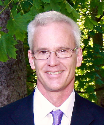
Speaker: Jeff Burns (IBM Thomas J. Watson Research Center, USA)
 Abstract:
Artificial Intelligence has recently become a major trend, driving the rapid development of new
compute capabilities. As AI functionality has improved, the demand for even greater
capabilities has grown, requiring significantly higher levels of performance and energy-
efficiency in the IT infrastructure. The maturation of classical semiconductor scaling has made
delivering these higher levels much more challenging; reliance on scaling alone is insufficient.
As a result, innovations in design, design automation, and architecture are crucial to improving
power-performance. Accelerators in heterogeneous systems will increasingly be needed to
improve overall system capabilities and power/performance. To enable practical accelerator
integration, system architectures must be designed to easily incorporate heterogeneous
components such as today’s GPUs, as well as future accelerators for cognitive applications.
Design processes must increase in efficiency to enable the cost-effective design of application-
specific accelerators. In this presentation, I will describe these trends, some exemplary
innovations that address them, and areas of future research towards heterogeneous systems
for the AI era.
Biography: Jeffrey L. Burns received his B.S. in Engineering from UCLA, and his M.S. and Ph.D. in Electrical Engineering from U.C. Berkeley. In 1988 he joined the IBM T.J. Watson Research Center and worked in layout automation and processor design. In 1996 he joined the IBM Austin Research Lab where he worked on the first 1 GHz PowerPC; he then managed the Exploratory VLSI Design group. In 2003 he returned to Watson to work on IBM Research’s annual study into the future of IT. He then managed a program exploring a streaming-oriented supercomputer. From mid-2005 until mid-2009 he managed the VLSI Design department, focusing on high-end processors, SoC designs, and 3D. From mid-2009 to September 2015 he was Director of VLSI Systems at Watson, and since September 2015 he has been Director, Systems Architecture and Design, managing the Division’s activities in VLSI design, design automation, microprocessor and systems architecture, and accelerator design.
Wednesday Keynote: January 24, 9:00-10:00 (Halla HALL)
Quality, Schedule and Cost: Design Technology and the Last Semiconductor Scaling Levers
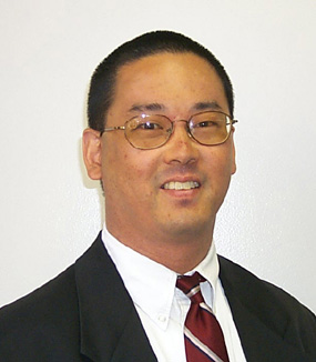
Speaker: Andrew B. Kahng (UCSD, USA)
 Abstract: Lateral scaling in semiconductor manufacturing and device architecture will be extremely challenging after the foundry 5nm/3nm nodes. Thus, continuing the Moore's-Law trajectory of value scaling will require new (and perhaps final) levers. There are three basic types of such levers. The first is quality: improved design tools and methods must recover IC design quality that was left on the table as the industry rode scaling in the past decade's "race to the end of the roadmap". The second is schedule: the temporal axis of Moore's Law (i.e., "one week is one percent") must become a focus for delivery of new, "design-based equivalent scaling" value. The third is cost: new mechanisms must be found to reduce the cost of IC design infrastructure as well as the cost and difficulty of the IC design process itself. In this talk, I will describe these levers and how the EDA community can contribute to their realization for future semiconductor design.
Biography: Andrew B. Kahng is Professor of CSE and ECE at UC San Diego, where he holds the endowed chair in High-Performance Computing. He has served as visiting scientist at Cadence (1995-1997) and as founder/CTO at Blaze DFM (2004-2006). He is the coauthor of 3 books and over 400 journal and conference papers, holds 33 issued U.S. patents, and is a fellow of ACM and IEEE. He has served as general chair of DAC, ISQED, ISPD and other conferences. He served as international chair/co-chair of the Design technology working group, and of the System Integration focus team, for the International Technology Roadmap for Semiconductors (ITRS) from 2000-2016. His research interests include IC physical design and performance analysis, the IC design-manufacturing interface, combinatorial algorithms and optimization, and the roadmapping of systems and technology.
Thursday Joint Keynote on "Memory": January 25, 8:30-10:00 (Halla HALL)
CAE challenge on High Capacity/High Bandwidth Memory Design
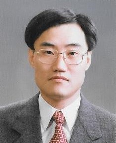
Speaker: Woojong Han (SK Hynix, Korea)
 Abstract:
It is a strong trend that the demand on high capacity and high bandwidth memory solutions are increasing continuously due to higher demand on hyper-scale data center and new emerging applications such as Machine Learning. Traditionally memory design relies heavily on custom circuit design, which makes general high-level synthesis and auto P&R much less efficient than SoC design. However due to ever increasing design and validation time as of complex, high speed memory devices, there is strong need on more efficient CAE capability that can combine the digital logic design and implementation method along with layout-based schematic design. At the same time the designer needs more accurate and efficient verification environment. There is significant effort on reducing the validation time without sacrificing coverage. To cope with critical timing margin issue on high bandwidth memory, statistical design environment is being developed, which can provide better correlation between real implementation and simulation. Also integrated design and validation environment is to be used to get integrated SI with On/Off-chip interface. We can also discuss about collaboration with customer who owns the platform.
Biography:
- 2016 – today: SVP of SK hynix, Head of Memory system R&D. Led effort on managed DRAM solution for higher capacity DIMM while with DRAM development group
- 2002 – 2016: Intel Corporation, SoC and platform architect working on various chipsets and controllers
- 2000 – 2002: API Networks, IO system architect working on IO subsystem based on HyperTransport technology
- 1986 – 2000: ETRI, Principal engineer leading several server system development projects including large scale parallel processing system with custom crossbar solution
TeraByte/s Bandwidth 2.5D HBM (High-bandwidth Memory Module) Designs for Deep Learning Artificial Intelligent Servers
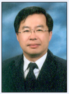
Speaker: Joungho Kim (KAIST, Korea)
 Abstract:
Recently, we are facing a newly emerging technology and industrial transition, named as 4th Industrial Revolution, which is based big data platforms, deep learning algorithms, and high performance GPU computing machines. Accordingly, demands for terabyte/s bandwidth GPU-DRAM computing performance are rapidly increasing. However, continuously growing gaps between GPU performance and DRAM data bandwidth are becoming the critical drawbacks. In order to meet the required terabyte/s bandwidth needs, we are proposing a novel High bandwidth memory (HBM) solution using TSV and Si interposer technologies.
In this presentation, we will introduce the basic approaches and designs of terabyte/s bandwidth 2.5D HBM (High-bandwidth Memory Module), in particular, which will be useful for deep learning artificial intelligent servers. Especially, we will talk about the signal and power integrity design, simulation methods, analysis results of TSV and Si interposer channels, including GPU-DRAM channels, and high-speed serial channels. In addition, we will discuss PDN impedance, and decoupling capacitor schemes as well. Finally, we will propose next generation HBM designs using active interposer and equalization schemes to even increase the bandwidths with lower power consumptions.
Biography: Dr. Joungho Kim received B.S. and M.S. degrees in electrical engineering from Seoul National University, Seoul, Korea, in 1984 and 1986, respectively, and Ph.D degree in electrical engineering from the University of Michigan, Ann Arbor, in 1993. In 1994, he joined Memory Division of Samsung Electronics, where he was engaged in Gbit-scale DRAM design. In 1996, he moved to KAIST. He is currently professor at electrical engineering department of KAIST. Also, he is director of 3DIC-RC (3DIC Research Center) supported by SK Hynix Inc, and SAE-RC (Smart Automotive Electronics Research Center) supported by KET Inc. Since joining KAIST, his research centers on EMC modeling, design, and measurement methodologies of 3D IC, TSV, Interposer, System-in-Package, multi-layer PCB, and wireless power transfer (WPT) technologies. Especially, his major research topic is focused on chip-package-PCB co-design and co-simulation for signal integrity, power integrity, ground integrity, timing integrity, and radiated emission in 3D IC, TSV and Interposer. He has authored and co-authored over 480 technical papers published at refereed journals and conference proceedings. Also, he has given more than 263 invited talks and tutorials at the academia and the related industries. He received Technology Achievement Award from IEEE Electromagnetic Society in 2010. He is IEEE fellow.