

Sponsored by:
Supported by:


Supporter's Exhibition:


|
|
|

| |
|---|---|
|
|
|
Supported by:
Supporter's Exhibition:
Tutorials
ASP-DAC 2019 offers attendees a set of three-hour intense introductions to specific topics. If you register for tutorials, you have the option to select two out of the nine topics. (This year, each tutorial will be presented once.)
- Date: Monday, January 21, 2019 (9:30-17:00)
| Room Saturn |
Room Uranus |
Room Venus |
Room Mars |
Room Mercury |
|
| 9:30 - 12:30 | Tutorial-1 Integrating Hardware and Algorithm Advances for Cognitive Systems |
Tutorial-2 Enablement of No-Human-in-the-Loop IC Design: Status and Directions |
Tutorial-3 Energy-Efficient Processing and Machine Learning at the Edge: from Sensing to Sensemaking |
Tutorial-4 Design for Reliability in the Nano-CMOS Era: New Holistic Methodologies for Reliability Modeling and Optimization |
Tutorial-5 Machine Learning in Test |
| 14:00 - 17:00 | Tutorial-6 Recent Development and Future Perspective of Quantum Annealing |
Tutorial-7 Embedded Heterogeneous Computing: Architectural Landscape and Software Challenges |
Tutorial-8 Smart Image Sensor Systems |
Tutorial-9 Machine Learning for Reliability of ICs and Systems |
Tutorial-1: Monday, January 21, 9:30 - 12:30 @Room Saturn
Integrating Hardware and Algorithm Advances for Cognitive Systems
- Organizer:
- Hai Li (Duke University)
- Speakers:
- Kaushik Roy (Purdue University)
- Hai Li (Duke University)
Abstract:
As big data processing becomes pervasive and ubiquitous in our lives, the desire for embedded-everywhere and human-centric information processing calls for cognitive computing paradigm that is capable of handling large volume of data dynamically according to environmental conditions, under limited hardware resources. This demand, however, is unlikely to be satisfied through the traditional hardware and software solutions. The performance of existing computer systems is greatly hindered by the increasing performance gap between CPU and memory as well as the fast-growing power consumption, while most practice on deep learning algorithms still heavily relies on large volume of labeled data. The integrated approaches that combine novel circuit/architecture with algorithm advances emerge as one of the most important and active area in computer and computing societies. The objective of the tutorial is to give a comprehensive overview on the status of cognitive computing systems, with a particular focus on the hardware design and system implementation as well as the evolution of neural network algorithms. The research studies on conventional platform as well as the neuromorphic system based on emerging nanotechnologies will be introduced. New applications and challenges will be discussed. The materials particular emphases the technical interactions between circuit design, device characteristics, and computing systems in order to provide a comprehensive overview to the attendees with various backgrounds and interests and maximize the benefits to design and EDA communities.Biography:
 Prof. Kaushik Roy joined the electrical and computer engineering faculty at Purdue University, West Lafayette, IN, in 1993, where he is currently Edward G. Tiedemann Jr. Distinguished Professor. His research interests include neuromorphic computing, device-circuit co-design for nano-scale Silicon and non-Silicon technologies, low-power electronics for portable, and new computing models enabled by emerging technologies. Dr. Roy has published more than 700 papers in refereed journals and conferences, holds 15 patents, supervised 75 PhD dissertations, and is co-author of two books on Low Power CMOS VLSI Design (John Wiley & McGraw Hill). Dr. Roy received the National Science Foundation Career Development Award in 1995, IBM faculty partnership award, ATT/Lucent Foundation award, 2005 SRC Technical Excellence Award, SRC Inventors Award, Purdue College of Engineering Research Excellence Award, Humboldt Research Award in 2010, 2010 IEEE Circuits and Systems Society Technical Achievement Award (IEEE Charles Doeser award), Distinguished Alumnus Award from Indian Institute of Technology (IIT), Kharagpur, Fulbright-Nehru Distinguished Chair, DoD Vannevar Bush Faculty Fellow Faculty Fellow (2014-2019), Semiconductor Research Corporation Aristotle award in 2015, and many best paper awards in international conferences and IEE journals. Dr. Roy was a Purdue University Faculty Scholar (1998-2003). He was a Research Visionary Board Member of Motorola Labs (2002) and held the M. Gandhi Distinguished Visiting faculty at Indian Institute of Technology (Bombay) and Global Foundries visiting Chair at National University of Singapore. He has been in the editorial board of IEEE Design and Test, IEEE Transactions on Circuits and Systems, IEEE Transactions on VLSI Systems, and IEEE Transactions on Electron Devices. He was Guest Editor for Special Issue on Low-Power VLSI in the IEEE Design and Test (1994) and IEEE Transactions on VLSI Systems (June 2000), IEE Proceedings – Computers and Digital Techniques (July 2002), and IEEE Journal on Emerging and Selected Topics in Circuits and Systems (2011). Dr. Roy is a fellow of IEEE.
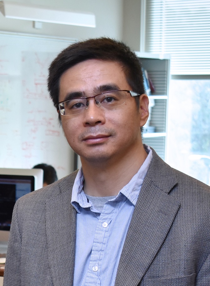
 Prof. Hai (Helen) Li is Clare Boothe Luce Associate Professor of Electrical and Computer Engineering Department at Duke University, USA. She works on hardware/software co-design for accelerating machine learning, brain-inspired computing systems, and memory architecture and optimization. She has authored or co-authored more than 200 technical papers in these areas and has authored a book entitled Nonvolatile Memory Design: Magnetic, Resistive, and Phase Changing (CRC Press, 2011). Dr. Li serves as an Associate Editor of IEEE TVLSI, IEEE TCAD, ACM TODAES, IEEE TMSCS, IEEE TECS, IEEE CEM, and IET-CPS. She has served as organization committee and technical program committee members for over 30 international conference series. Dr. Li is a recipient of the NSF CAREER Award (2012), the DARPA Young Faculty Award (2013), TUM-IAS Hans Fisher Fellowship from Germany (2017) and seven best paper awards. Dr. Li is a senior member of IEEE and a distinguished member of ACM, a distinguished speaker of ACM (2017-2020), and a distinguished lecture of IEEE CAS society (2018-2019). More about her is available at: https://cei.pratt.duke.edu/
Tutorial-2: Monday, January 21, 9:30 - 12:30 @Room Uranus
Enablement of No-Human-in-the-Loop IC Design: Status and Directions
- Organizer:
- Andrew B. Kahng (University of California, San Diego)
- Speakers:
- David White, Senior (Cadence Design Systems, Inc.)
- Shankar Sadasivam (Qualcomm Inc.)
- Andrew B. Kahng (University of California, San Diego)
Abstract:
The semiconductor ecosystem faces a design crisis: design at leading nodes faces growing barriers of cost, expertise, and risk. Due to these barriers, system innovation cannot access the latest semiconductor technologies, and this jeopardizes the health of the entire industry ecosystem of design, EDA, and process. To mitigate the design crisis, leading players across the fabless, EDA and foundry sectors – as well as academic researchers – are aggressively exploring big-data / machine learning based approaches that can reduce human effort and schedule requirements of IC design.Recently, the U.S. Defense Advanced Research Projects Agency (DARPA) has launched a new program, called “IDEA”, that attacks cost and schedule barriers in IC design via “no-human-in-the-loop”, 24-hour layout automation flows – including the RTL-to-GDSII flow that is central to IC implementation. Commercial EDA tools have been driven by leading customers to squeeze as much design quality (PPA) from the foundry enablement as possible. By contrast, the IDEA program proposes to drive EDA tool development in a different direction: “no-human-in-the-loop” returns the focus to “automation”, trading away PPA in return for autonomous, “self-driving tools”, along with schedule reductions.
This tutorial will summarize key elements in the road toward “no-human-in-the-loop” IC design, including current status and near-term directions.
Machine learning and decision-making: To achieve “no-human-in-the-loop”, it is necessary to understand where and why humans are in the loop of IC design today (e.g., in floorplanning, power planning, clock distribution, and timing closure steps). Wherever human expertise and decision-making is critical to design success today, it must be modeled and automated.
Dr. Shankar Sadasivam of Qualcomm (possibly, joined by his colleague Dr. Rajeev Jain) will discuss machine learning theory for decision-making, with subtopics including reinforcement learning, multi-arm and contextual bandits, Bayesian optimization, and online learning. Dr. Sadasivam will also walk through applications of these techniques in the SOC design context.
Characterization and leverage of design intent: One of the keys to fully automating the full design flow is to build technology to characterize design intent and to map it to physical design decisions at the chip, package and board levels. The key technologies to making this work include machine learning, analytics, and visualization algorithms. In this part of the tutorial, Dr. David White of Cadence will review some of the critical algorithms and visualization tools, as well as explore the available synergies between the EDA and design communities regarding use models that facilitate intent-driven design and simulation.
Data for learning: Automation and machine learning must broadly advance in two directions: (1) modeling and prediction of downstream flow outcomes (e.g., routing success, hold buffer insertion, post-timing closure block area) to avoid loops in the flow, and to provide optimization objectives at early flow stages; and (2) modeling of systematic discrepancies between approximate analyses (PEX, STA, etc.) and “signoff-quality” analyses, to reduce analysis errors that must be covered by design guardbands.
Prof. Andrew Kahng of UCSD will present a roadmap along which the EDA and IC design communities can progress in these directions. Crucially, the design, EDA and research communities must share responsibility for overcoming the “small, expensive data” challenge that hampers development of machine learning models for IC design. A standard methodology for “metrics” collection during the design process, as a prerequisite to development of machine learning models, will be described along with recent example experiences and use cases.
As time permits, the three tutorial presenters will add discussion on further topics such as (1) examples of machine learning infrastructure deployed by design organizations; (2) collaborative working models between EDA vendors and customers; and (3) leverage of open-source code and elastic cloud resources.
Biography:
 David White received a Doctor of Science Degree in Electrical Engineering and Computer Science from the Massachusetts Institute of Technology in 2001. Dr. White is currently a Senior Group Director of R&D at Cadence Design Systems. He joined Cadence in 2006 through the acquisition of Praesagus, a software company he co-founded in 2001 and where he served as CTO. Prior to that he co-founded and led Neurodyne in 1991, which provided machine learning software technology for the industrial and aerospace industries. He also worked in the McDonnell/Boeing New Aircraft Products Division on machine learning applications for aerospace and related manufacturing technologies. Dr. White has served as a member of the Advisory Board for the National Science Foundation in Washington D.C. and the MIG Advisory Board at MIT. He was an editor and co-author of the Handbook of Intelligent Control, a text written in 1992 by many of the pioneers in the field of machine learning. Since 1990, he has given invited talks at OSTP and NSF forums, as well as IEEE, NASA, ACM and IJCNN conferences. He has most recently given keynote and invited talks on machine learning at CASPA, IEEE EDPS as well as Design Con 2017 and 2018. He has over 30 issued patents in the areas of electronic design and machine learning.
 Shankar Sadasivam received the B.Tech. degree in Electrical Engineering from the Indian Institute of Technology (IIT), Madras, in 2005, and the M.S. and Ph.D. degrees in Electrical and Computer Engineering from the University of Illinois at Urbana-Champaign (UIUC), in 2008 and 2011, respectively. His PhD dissertation focused on developing Machine Learning approaches to traditional signal processing problems in information hiding. Since 2011, he has been with Qualcomm where he has been driving various Machine Learning research and product initiatives, e.g., the Always-On Mobile Contextual Awareness project, where his team designed novel Machine Learning algorithms and architectures for always-On contextual awareness usecases. Currently, he leads Machine Learning R&D to maintain Qualcomm’s leadership in cost, features and power for mobile chipset platforms across multiple product lines, in the face of exponentially increasing product complexity with deep-submicron Moore's law scaling.
 Andrew B. Kahng is Professor of CSE and ECE at UC San Diego, where he holds the endowed chair in High-Performance Computing. He has served as visiting scientist at Cadence (1995-1997) and as founder/CTO at Blaze DFM (2004-2006). He is the coauthor of 3 books and over 400 journal and conference papers, holds 34 issued U.S. patents, and is a fellow of ACM and IEEE. He has served as general chair of DAC, ISQED, ISPD and other conferences. He served as international chair/co-chair of the Design technology working group, and of the System Integration focus team, for the International Technology Roadmap for Semiconductors (ITRS) from 2000-2016. His research interests include IC physical design and performance analysis, the IC design-manufacturing interface, combinatorial algorithms and optimization, and the roadmapping of systems and technology. Starting June 2018, he serves as principal investigator of “OpenROAD”, an $11.3M U.S. DARPA project aimed at developing open-source, autonomous (“no humans”) tools for IC/hardware implementation.
Tutorial-3: Monday, January 21, 9:30 - 12:30 @Room Venus
Energy-Efficient Processing and Machine Learning at the Edge: from Sensing to Sensemaking
- Organizer and Speaker:
- Massimo Alioto (National University of Singapore)
Abstract:
The Internet of Things (IoT) is now taking off as new technology wave in the semiconductor industry. The IoT is currently posing several challenges at its edge, in view of the strict requirements in terms of miniaturization, cost and lifetime of the distributed sensors (“IoT nodes”) that constitute its physical interface. Being relatively incompressible, the large wireless power associated with radios is generally mitigated by making IoT nodes smarter, hence reducing communications with the cloud. To retain the advantages of pushing significant processing into the IoT nodes, ultra-low energy processing needs to be achieved by leveraging multiple design dimensions, ranging from energy-performance scaling (e.g., wide voltage scaling), to energy-quality scaling (e.g., adjustable accuracy), and application specific accelerators for data sensemaking (e.g., machine learning engines).In this tutorial, a survey of fresh ideas and recent techniques to design ultra-low energy circuits for in-node processing in IoT applications is presented. A preliminary analysis of the current status of the IoT and trends in the foreseeable future are introduced to understand the system constraints, and translate them into design specifications. Then, minimum-energy operation is discussed by introducing near-threshold CMOS logic circuits along with their unique properties and challenges, while debunking several wrong assumptions stemming from traditional above-threshold low-power common wisdom. Practical design guidelines are also provided for near-threshold standard cell libraries, clock networks, memories, and other aspects related to automated design. For the first time, a novel variation-aware design framework is presented to quickly estimate the typically large design margin imposed by process/voltage/temperature variations, and guide the design to reduce the design margin.
As crucial building block of IoT nodes with on-chip sensor data sensemaking, energy-efficient accelerators for machine learning are introduced, building on the above circuit-level techniques. As particularly important case, low-energy deep learning accelerators are discussed by highlighting the “big ideas” that are enabling the recent and very rapid improvements in energy efficiency. Concepts are exemplified by integrated prototypes from industry and academia.
Biography:
 Massimo Alioto is with the ECE Department of the National University of Singapore, where he leads the Green IC group and the Integrated Circuits and Embedded Systems area. Previously, he held positions at the University of Siena, Intel Labs – CRL (2013), University of Michigan - Ann Arbor (2011-2012), University of California – Berkeley (2009-2011), EPFL - Lausanne.
He is (co)author of 250+ publications, and three books with Springer. His primary research interests include ultra-low power VLSI circuits and systems, self-powered nodes, near-threshold circuits for green computing, widely energy-scalable integrated systems, hardware security, and emerging technologies.
Prof. Alioto is the Editor in Chief of the IEEE Transactions on VLSI Systems (2019 onwards), and Deputy Editor in Chief of the IEEE Journal on Emerging and Selected Topics in Circuits and Systems. He was the Chair of the “VLSI Systems and Applications” Technical Committee of the IEEE CASS, and Distinguished Lecturer. He also serves or has served as Associate Editor of several journals. He served as Guest Editor of numerous journal special issues, Technical Program Chair of several IEEE conferences (ISCAS 2022, SOCC, PRIME, ICECS, VARI, NEWCAS, ICM), Track Chair (ICCD, ISCAS, ICECS, VLSI-SoC, APCCAS, ICM), and TPC member (ISSCC, ASSCC). He is currently member of the IEEE CASS Board of Governors, and an IEEE Fellow.
Massimo Alioto is with the ECE Department of the National University of Singapore, where he leads the Green IC group and the Integrated Circuits and Embedded Systems area. Previously, he held positions at the University of Siena, Intel Labs – CRL (2013), University of Michigan - Ann Arbor (2011-2012), University of California – Berkeley (2009-2011), EPFL - Lausanne.
He is (co)author of 250+ publications, and three books with Springer. His primary research interests include ultra-low power VLSI circuits and systems, self-powered nodes, near-threshold circuits for green computing, widely energy-scalable integrated systems, hardware security, and emerging technologies.
Prof. Alioto is the Editor in Chief of the IEEE Transactions on VLSI Systems (2019 onwards), and Deputy Editor in Chief of the IEEE Journal on Emerging and Selected Topics in Circuits and Systems. He was the Chair of the “VLSI Systems and Applications” Technical Committee of the IEEE CASS, and Distinguished Lecturer. He also serves or has served as Associate Editor of several journals. He served as Guest Editor of numerous journal special issues, Technical Program Chair of several IEEE conferences (ISCAS 2022, SOCC, PRIME, ICECS, VARI, NEWCAS, ICM), Track Chair (ICCD, ISCAS, ICECS, VLSI-SoC, APCCAS, ICM), and TPC member (ISSCC, ASSCC). He is currently member of the IEEE CASS Board of Governors, and an IEEE Fellow.
Tutorial-4: Monday, January 21, 9:30 - 12:30 @Room Mars
Design for Reliability in the Nano-CMOS Era: New Holistic Methodologies for Reliability Modeling and Optimization
- Organizers and Speakers:
- Sheldon Tan (University of California, Riverside)
- Hussam Amrouch (Karlsruhe Institute of Technology)
Abstract:
Reliability has become a significant challenge for design of current nanometer integrated circuits (ICs). Long-term reliability degradation caused by aging effects are becoming limiting constraints in emerging computing and communication platforms due to increased failure rates from the continuous transistor scaling, increasing process variations and aggressive power reductions. Reliability problems will get worse as future chips will show signs of aging much faster than the previous generations. Despite aging occurs at the physical level, workloads at the system level play a major role in stimulating the underlying mechanisms of aging. Therefore, holistic solutions in which the physical effects are linked with and abstracted all the way up to the system level become necessary for mitigating the looming reliability crisis.The motivation of this tutorial is to understand the newest research results in reliability from ground up in which both Bias Temperature Instability (BTI) and Electromigration (EM), which are the key aging mechanisms in transistors and interconnect wires, are jointly covered. Intended audiences are circuit- and system- level designers who investigate reliability aspects in embedded systems.
Talk 1: EM-Aware Design: from Physics to System Level
Speaker: Sheldon Tan
In this talk, we will present some of recent research works in my research lab (VSCLAB) at UC Riverside. First, we will review a recently proposed physics-based three-phase EM models for multi-segment interconnect wires, which consists of nucleation, incubation and growth phases to completely model the EM failure processes in typical copper damascene interconnects. The new EM model can predict more accurate EM failure behaviors for multi-segment wires such as interconnects with reservoir and sink segments. Second, we will present newly proposed fast aging acceleration techniques for efficient EM failure detections and validation of practical VLSI chips. We will present the novel configurable reservoir/sink-structured interconnect designs in which the current in the sink segment can be activated/deactivated dynamically during operation. In this way, the stress conditions of the interconnect wires can be increased and the lifetime of the wires can be reduced significantly. Afterwards, we will present the compact dynamic EM models for general multi-segment interconnect wires and voltage-based EM immortality check algorithm for general interconnect trees. Then we will present a fast 2D stress numerical analysis technique based on the Krylov subspace and finite difference time domain methods (FDTD) for general interconnect wires structure. The proposed numerical analysis method can lead to 100X speedup over the simple FDTD method and can be applied to any interconnect structures for all the EM wear-out phases. Last, not least, we will focus on the system level dynamic reliability management (DRM) techniques based on the newly proposed physics-based EM models. We will show several recent works of the EM-aware DRM for lifetime optimizations for dark-silicon, embedder/real-time systems and 3D ICs to improve the TSV reliability.
Talk2: Estimating and Optimizing BTI Effects: from Physics to System Level
Speaker: Hussam Amrouch
In this presentation, we will first demonstrate how we can bring aging awareness to existing EDA tool flows based on so-called degradation-aware cell libraries. We will show why these libraries are necessary not only to accurately estimate guardbands but to efficiently containing them. Then, we will show how these libraries can be used within the standard tool flows to quantify the impact of aging at the system level in the context of image processing. Afterwards, we will demonstrate how aging-induced timing errors can be converted into deterministic and controlled approximations instead. This enables designers to narrow or even remove guardbands through exploring application of approximate computing principles in the context of aging. Finally, we will demonstrate how the existing view of BTI needs to be updated. State of the art used to assume BTI as a long-term reliability degradation that needs months and years to appear. However, in the deep nano technology, BTI has shifted to a short-term reliability challenge. We will explain why embedded system designers need to take that into account when designing guardbands. Otherwise, reliability cannot be sustained at runtime. At the end of our presentation, we will distribute to attendees USB sticks, which contain our degradation-aware libraries. This will enable them to study BTI effects using existing commercial EDA tool flows.
Biography:
 Sheldon Tan received Ph.D. degree in electrical and computer engineering from the University of Iowa, Iowa City, in 1999. He is a Professor in the Department of Electrical and Computer Engineering, University of California, Riverside, CA. He also is a cooperative faculty member in the Department of Computer Science and Engineering at UCR. His research interests include VLSI reliability modeling, optimization and management at circuit and system levels, hardware security, thermal modeling, optimization and dynamic thermal management for many-core processors, parallel computing and adiabatic and Ising computing based on GPU and multicore systems. He has published more 280 technical papers and has co-authored 5 books on those areas. Dr. Tan received NSF CAREER Award in 2004. He also received three Best Paper Awards from ASICON’17, ICCD'07, DAC’09. He also received the Honorable Mention Best Paper Award from SMACD’18. He was a Visiting Professor of Kyoto University as a JSPS Fellow from Dec. 2017 to Jan. 2018. He is now serving as Editor in Chief for Elsevier’s Integration, the VLSI Journal, the Associate Editor for three journals: IEEE Transaction on VLSI Systems (TVLSI), ACM Transaction on Design Automation of Electronic Systems (TODAE) and Elsevier’s Microelectronics Reliability.
 Hussam Amrouch is a Research Group Leader at the Chair for Embedded Systems (CES), Karlsruhe Institute of Technology (KIT), Germany. He is leading of the Dependable Hardware research group. He received his Ph.D. degree from KIT in 2015 with distinction (summa cum laude). His main research interests are design for reliability, thermal-aware VLSI design, modeling and mitigating aging effects at the device and circuit levels. He holds six HiPEAC Paper Awards. He has recently three best paper nominations at DAC'16, DAC'17 and DATE'17 for his work on reliability. He currently serves as Associate Editor at Integration, the VLSI Journal.
Tutorial-5: Monday, January 21, 9:30 - 12:30 @Room Mercury
Machine Learning in Test
- Organizer and Speaker:
- Yu Huang (Mentor, A Siemens Business)
Abstract:
Machine learning has become a very hot topic in recent years due to its successful application in diverse areas such as computer vision, natural language processing, and intelligent gaming. Exciting new applications, such as autonomous driving, robotics, and AI assisted medical diagnosis, continue to emerge on a regular basis. However, machine learning has still not made much headway in the area of IC testing, since most researchers are unfamiliar with the underlying theory and algorithms, and are unsure of how to apply these techniques in the test domain. We believe machine learning is a powerful and innovative new technology, and can make a significant difference in the area of testing in the near future. This tutorial will review the basics of machine learning, its applications in testing, and forecast future applications of machine learning in testing. It will include the following two parts that are presented in an interleaving manner around each topic:In the first part, we will provide the background necessary to understand the applications of machine learning in testing. We will start by covering the basics of machine learning. We will also give a brief overview of deep learning. We will end by showing how easy it is to try using machine learning and deep learning models, thanks to powerful, free libraries. We will start by characterizing what machine learning is: its definition, supervised vs unsupervised learning, classification vs regression problems. We will then introduce the notion of an objective or loss function. Using examples, we will show how our intuition about probability naturally leads to maximum likelihood estimation. We will proceed to take a deeper dive into regression. We will start by looking at simple linear regression. We will describe polynomial regression and show how even a simple linear model can be used to obtain a non-linear prediction by leveraging higher level features - a theme which we will keep revisiting throughout the tutorial. This will lead us to one of the pitfalls of machine learning - overfitting. We will discuss two easy and practical ways to avoid overfitting: regularization and cross validation. Our next focus will be classification. We will talk about a popular classifier: Support Vector Machines (SVMs). We will introduce the kernel trick which transforms an SVM into a powerful classifier. We will discuss how the concept of maximum margin separation, which is the key concept underlying an SVM, can be extended to regression to obtain the Support Vector Regression algorithm. We will motivate Bayes Theorem using examples and make a brief foray into the world of conditional probability and Bayesian Inference. We will describe the extremely powerful framework of Probabilistic Graphical Models and show how Bayes Theorem is at its foundation. Next, we will spend some time on the hottest sub-field in machine learning: deep learning. We will start by describing neural networks. We will discuss the reasons why they were not popular or in much use till a few years ago. We will introduce deep learning and talk about the theoretical and practical breakthroughs that happened a decade earlier which led to its meteoric rise. We will look at examples where deep learning has been used effectively, and the challenges it Submitted to TTTC TTEP 2018 currently faces. We will also discuss how deep learning researchers are trying to overcome these challenges. To conclude this part, we will mention freely downloadable Python libraries and show some actual python code. We hope to drive home how easy it is to try traditional as well as state-of-the-art machine learning / deep learning models and algorithms.
In the second part of the tutorial, we will start by reviewing published work in testing, where machine learning algorithms are used to solve hard problems. These problems will encompass the following areas of testing:
1. Yield learning / root cause analysis
With decreasing feature sizes and increasing complexity of fabrication processes for manufacturing VLSI semiconductor devices, more systematic defects occur at the advanced technology nodes. Product yield ramp up is mostly determined by how fast systematic defects are identified and fixed. Given the large amount of time and resources needed for doing physical failure analysis (PFA), it is becoming infeasible to find systematic defects by doing PFA on a large number of failing devices. For this reason, volume diagnosis data mining, where we apply statistical and machine learning models to a collection of diagnosis reports, is being increasingly used for root cause identification. This greatly reduces the turnaround time and cost of systematic defect identification. The root cause information can be used to do yield analysis and provide guidance on how to improve yield. In addition, it can be used to reduce PFA cost by focusing on failing devices with systematic defects.
2. Diagnosis
If a defect can be modeled as a permanent fault, simulating the fault can help us identify the suspects. However, real defects on Silicon are very complicated, and might not be permanent. We will use scan chain failure diagnosis as an example, and focus on handling hard-to-model defect behaviors. We will explain a machine learning based diagnosis algorithm that was implemented in a commercial tool.
3. DFT planning
Various configuration choices are available for decompression and compaction hardware. Finding an optimal configuration is very tedious and time consuming if we use a brute force approach. Using machine learning, this problem can be solved efficiently and effectively. Next, we will discuss which characteristics of test, diagnosis, and DFT applications are deep-learning friendly, and which are not. We will also provide advice on how to select applications that might be solved effectively using deep learning. Finally, we will propose future research directions in the area of testing, where we think machine learning (especially deep learning) can make a big impact.
Biography:
 Dr. Yu Huang is a Principal Engineer in the Silicon Test Systems Division of Mentor, A Siemens Business. His research interests include VLSI SoC testing, ATPG, compression and diagnosis. He holds 27 US patents and has 9 more patents pending. He has published more than 100 papers in leading IEEE Journals, conferences and workshops. He is a senior member of the IEEE. He has served as technical program committee member for DAC, ITC, ATS, ETS, ASPDAC, NATW and other conferences and workshops in the testing area. He received a Ph.D. from the University of Iowa in 2002.
Tutorial-6: Monday, January 21, 14:00 - 17:00 @Room Saturn
Recent Development and Future Perspective of Quantum Annealing
- Organizer:
- Shu Tanaka (Waseda University)
- Speakers:
- Shu Tanaka (Waseda University)
- Yoshiki Matsuda (Fixstars Corporation)
- Kotaro Tanahashi (Recruit Communications Co., Ltd.)
- Yuya Seki (National Institute of Advanced Industrial Science and Technology, Japan)
Abstract:
Quantum annealing is expected to be a promising calculation method to perform the combinatorial optimization efficiently, which is a kind of natural computing technology using quantum phenomena. Quantum annealing was proposed as an alternative heuristic algorithm of simulated annealing in the background of statistical physics. In the simulated annealing, we introduce the temperature and decrease it gradually, whereas in the quantum annealing we introduce a quantum effect and decrease it gradually. Based on the theoretical proposition of quantum annealing, the first commercial quantum annealing machine was released in 2011. After that, D-Wave has been developed step by step, that is, the number of qubits in D-Wave is doubling every two years. In addition, hardware development, middleware/software development, application search of quantum annealing and its cousin technologies have been done by quite a few research groups. In this tutorial, the theoretical background of quantum annealing will be shown. In addition, very recent development of hardware, middleware/software, and application search of quantum annealing will be explained.(1) Recent Development and Future Perspective of Quantum Annealing
In this tutorial, historical review and theoretical background of quantum annealing will be given. In addition, the procedure of quantum annealing will be explained. When we perform combinatorial optimizations by using quantum annealing machines, we have to prepare the Ising model which is a theoretical model in statistical physics. The structure of Ising model corresponds to the cost function of combinatorial optimization. In the first part of this tutorial, I will show some examples of the mapping from typical combinatorial optimization problems to the Ising model.
In the second part of this tutorial, I will explain the details of quantum annealing hardware. In existing quantum annealing hardware, superconducting qubits are arranged, and we embed the Ising model which corresponds to the combinatorial optimization problem we want to solve.
In the third of this tutorial, I will show some remaining problems in quantum annealing and its related technologies.
(2) Tutorial of Ising computations for combinatorial optimization problems
There exists a significant difference between the architectures of logic and Ising calculations, especially for the programming styles. The architecture of the Ising machine is suitable for describing the problem’s “goals” directly, while the instruction and operands are constructed by “solutions” for the conventional procedural programming style. The problem’s “goals” mean the relationships and preferable states among the Boolean variables.
The preferable state is expressed as the function which is called the energy (or cost/target) function for combinatorial optimization problems. For example, when we want to obtain the state “two variables are the same value” as a goal, we build the function with two variables inputs which takes the lowest (or highest) value when the goal, variables are the same value, is satisfied. The building of the energy function itself is the programming of the Ising machines.
In this tutorial, firstly we will show basic formulations of the energy function and the solving processes on the real Ising machines. Then, we will demonstrate our middleware between Ising machines and conventional programming languages, and we will explain some techniques to implement concrete examples of typical combinatorial optimizations to Ising machines. Finally, we will discuss further developments of Ising machines and software.
(3) Quantum Annealing for Machine Learning: Feature Selection and Sampling Applications
Optimizations play an essential role in many machine learning algorithms. However, some combinatorial optimization problems which belong to the NP-hard class cannot be solved efficiently by conventional optimization methods. Recently, quantum annealing (QA) has been shown to be effective for optimization problems in machine learning, such as feature selection or sampling problems.
In the first part of this tutorial, we will introduce a couple of feature selection algorithms optimized by quantum annealing machines. Feature selection, to find a subset of relevant features, is an important problem in machine learning both to speed up the training and to improve the generalization ability of the model. However, the number of combinations of the feature subset increases exponentially with the dimension size of the data. We introduce methods to formulate feature selection problem as Ising model to be solved by QA machines.
Next, we will discuss the applications of QA as a sampler. Some generative models in machine learning such as Boltzmann machines require samplings from the Boltzmann distributions. Since exact sampling from the distribution is intractable, we usually use heuristics such as Markov chain Monte Carlo methods (MCMC). Recent studies showed QA machines can accelerate the training of Boltzmann machines. We will introduce some potential applications of QA as a sampler.
(4) Beyond Transverse-Field Quantum Annealing
Performance improvement of quantum annealing (QA) is an important but unsolved issue. Although current implementations of QA use a uniform transverse field as driver Hamiltonian inducing quantum fluctuations, the transverse-field QA requires exponentially long time to solve certain problems. In this tutorial, recent approaches to improve the performance of QA are introduced.
Firstly, we explain how to estimate the performance of QA. In order to clarify discussion, we focus on quantum adiabatic computation (QAC) that is a procedure of quantum annealing satisfying the quantum adiabatic condition. From the statistical-mechanical point of view, quantum phase transition phenomenon is closely related to the performance of QA. In particular, quantum first order phase transition is symptom of the failure of QA.
Secondly, we introduce intractable problems for the transverse-field QA. Failure of QA is shown from both aspects of phase transition phenomenon and the quantum adiabatic condition.
Finally, we introduce successful attempts to improve the performance of QA. Except for special cases, QA requires exponentially long time to solve problems in which quantum first order phase transitions occur. Some methods to avoid the first order transitions are introduced. In addition, we explain a keyword "non-stoquasticity" related to the attempts.
Biography:
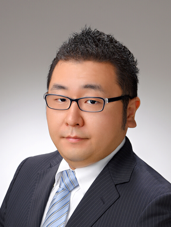 Shu Tanaka is an associate professor at Green Computing Systems Research Organization, Waseda University. He is also a PRESTO researcher, JST, a MITOU Target project manager, IPA, and an adviser at AI & Robotics committee, Mobile Computing Promotion Consortium. He received a Ph. D. in physics from the University of Tokyo in 2008. He got the 9th Award for the Encouragement of Young Physicists from the Physical Society of Japan in 2015. He wrote a pedagogical book on quantum annealing entitled, “Quantum Spin Glasses, Annealing and Computation” from Cambridge University Press in 2017. He has worked in fields of the theory of statistical physics, materials science, and Ising model-based computation including quantum annealing.
 Yoshiki Matsuda is a Lead Engineer at Fixstars corp, Japan. He is working on the next-generation computing solutions as a research engineer. His current interests include the middleware developments for Ising machines such as quantum annealing machines. He received a Ph.D. in physics from Tokyo Institute of Technology. Prior to joining Fixstars corp., he was a researcher of physics, and his profession was the field of numerical calculation of physics and statistical mechanics of Ising systems.
 Kotaro Tanahashi received a master’s degree in engineering from Kyoto University in 2015. He is currently working for Recruit Communications Co., Ltd. as a machine learning engineer. He is working on researches of the application of Ising annealing machines such as quantum annealing machines for digital marketing. He is also developing optimization engines for online advertising systems such as real-time bidding.
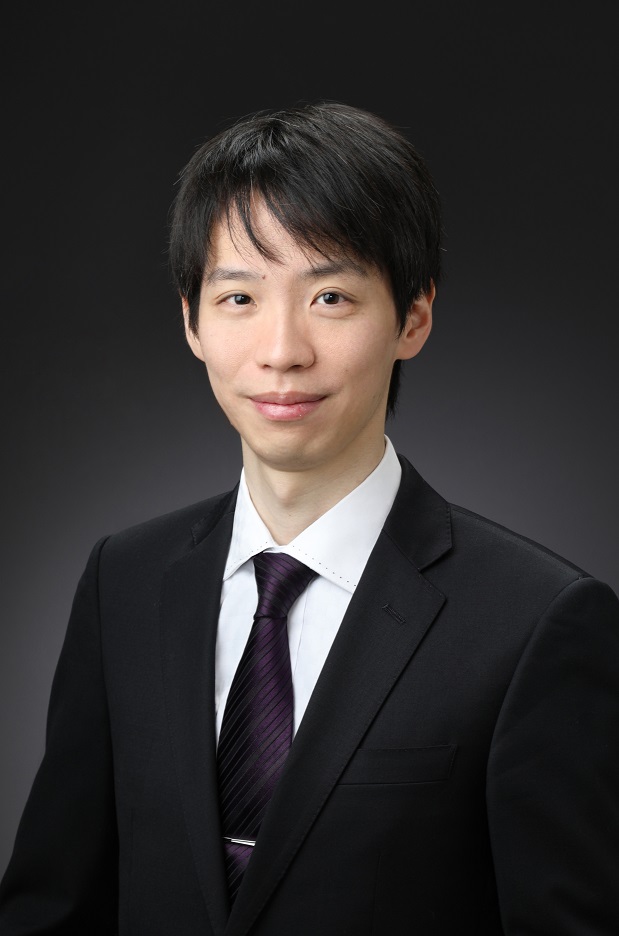
 Yuya Seki is a postdoctoral researcher at National Institute of Advanced Industrial Science and Technology, Japan. He received Ph.D. in physics from Tokyo Institute of Technology in 2016. His research focuses on quantum statistical mechanics for systems of quantum annealing, and improving the performance of quantum annealing.
Tutorial-7: Monday, January 21, 14:00 - 17:00 @Room Uranus
Embedded Heterogeneous Computing: Architectural Landscape and Software Challenges
- Organizer and Speaker:
- Tulika Mitra (National University of Singapore, Singapore)
Abstract:
Heterogeneous computing, materialized in the form of multiprocessor system-on-chips (MPSoC) comprising of various processing elements such as general-purpose cores with differing characteristics, GPUs, DSPs, non-programmable accelerators (e.g., AI accelerators), and reconfigurable computing, are expected to dominate the current and the future embedded and mobile platform landscape. The heterogeneity enables a computational kernel with specific requirements to be paired with the processing element(s) ideally suited to perform that computation, leading to substantially improved performance and energy-efficiency. While heterogeneous computing is an attractive proposition in theory, considerable software support at all levels is essential to fully realize its promises. The system software needs to orchestrate the different on-chip compute resources in a synergistic manner with minimal engagement from the application developers. This tutorial will put the spotlight on the architectural and software perspective of embedded heterogeneous computing, especially in the context of popular emerging applications, such as artificial intelligence, 3D gaming, multimedia processing and analytics. The tutorial will introduce the technology trends driving heterogeneous computing, provide an overview of computationally divergent and performance heterogeneous multi-cores, and present recent research in architecture, compiler, and runtime support to fully realize the potential of heterogeneity towards high-performance, energy-efficient computing. The topics covered by the tutorial include:- Technology trends behind heterogeneous computing
- Architectural landscape: performance heterogeneous CPU (e.g., ARM big.LITTLE), GPU, DSP, accelerators (e.g., Neural Processing Units), reconfigurable computing fabric
- Memory hierarchy for heterogeneous computing
- Software programmability challenges
- Application scheduling on heterogeneous computing systems
- Power and thermal Management for heterogeneous computing systems
Biography:
 Tulika Mitra is a Professor of Computer Science at School of Computing, National University of Singapore (NUS). Her research interests span various aspects of the design automation of embedded real-time systems with particular emphasis on energy-efficient computing, heterogeneous computing, application-specific processors, and software timing analysis/optimizations. She has authored over hundred and fifty scientific publications in leading international journals and conferences and holds multiple US patents. Her research has been recognized by best paper award and nominations in leading conferences. She is the recipient of the Indian Institute of Science Outstanding Woman Researcher Award and is an IEEE Distinguished Visitor. Prof. Mitra currently serves as Senior Associate Editor of the ACM Transactions on Embedded Computing Systems, Deputy Editor-in-Chief of IEEE Embedded Systems Letters, Associate Editor of IEEE Design & Test Magazine and EURASIP Journal on Embedded Systems. She has served as Associate Editor of IEEE TCAD in the past. She has served in the program committee of all major conferences in electronic design automation, embedded systems, and real-time systems including technical program chair of EMOSFT, CASES, and program vice-chair of ASPDAC.
Tutorial-8: Monday, January 21, 14:00 - 17:00 @Room Venus
Smart Image Sensor Systems
- Organizers and Speakers:
- Marilyn Wolf (Georgia Institute of Technology)
- Saibal Mukhopodhyay (Georgia Institute of Technology)
- Jong Hwan Ko (Agency for Defense Development, Korea)
Abstract:
The tutorial will cover:- Fundamentals of computer vision applications: detection, recognition, tracking.
- Computer vision methods: feature extraction algorithms, neural networks and machine learning.
- Algorithm/architecture co-design.
- Analog mixed-signal smart sensors.
- 3D smart sensor technology.
The second section will focus on on smart sensor architectures and systems. After reviewing the basics of CMOS APS image sensor design, the talk will discuss several approaches to integrated smart sensors. 3D smart sensors use back-side illuminated (BSI) sensors with front side connections to analog/digital conversion, memory, and processing. 3D architectures provide very high bandwidth to both the sensor and to memory. Computational architectures are fine-grained and support MIMD computation. These architectures support both high bandwidth to processors and memory as well as low latency. Thermal behavior must be carefully managed to avoid degrading both computational performance and image noise. Analog and digital techniques can be combined to provide low latency and low power.
Biography:
 Marilyn Wolf is Farmer Distinguished Chair in Embedded Computing Systems and GRA Eminent Scholar at the Georgia Institute of Technology. She received her BS, MS, and PhD in electrical engineering from Stanford University in 1980, 1981, and 1984. She was with AT&T Bell Laboratories from 1984 to 1989 and was on the faculty of Princeton University from 1989 to 2007. Her research interests include cyber-physical systems, Internet-of-Things, embedded computing, embedded computer vision, and VLSI systems. She has received the ASEE Terman Award and IEEE Circuits and Systems Society Education Award. She is a Fellow of the IEEE and ACM.
Saibal Mukhopadhyay received the bachelor of engineering degree in electronics and telecommunication engineering from Jadavpur University, Calcutta, India in 2000 and the Ph.D. degree in electrical and computer engineering from Purdue University, West Lafayette, IN, in August 2006. He joined the faculty of the Georgia Institute of Technology in September 2007. Dr. Mukhopadhyay worked at IBM T. J. Watson Research Center, Yorktown Heights, N.Y. as research staff member from August 2006 to September 2007 and as an intern in summers of 2003, 2004, and 2005. At IBM, his research primarily focused on technology-circuit co-design methodologies for low-power and variation tolerant static random access memory (SRAM) in sub-65nm silicon technologies. Dr. Mukhopadhyay has (co)-authored over 60 papers in reputed conferences and journals and filed four United States patents.
 Jong Hwan Ko received double B.S. degrees in computer science and engineering and mechanical and aerospace engineering from Seoul National University, where he received the M.S. degree in electrical engineering and computer science. He received Ph.D. degree in electrical and computer engineering at Georgia Institute of Technology in August 2018. He worked at Microsoft AI and Research as a research intern in 2017. He is currently a senior researcher at the Agency for Defense Development (ADD) in Korea, and he will join SungKyunKwan University (SKKU) as an assistant professor from March 2019. His research interests include robust and efficient deep learning techniques, audio and image processing, and low-power Internet-of-Things systems design. He has received the Best Paper Award at the International Symposium on Low Power Electronics and Design (ISLPED) in 2016.
Tutorial-9: Monday, January 21, 14:00 - 17:00 @Room Mars
Machine Learning for Reliability of ICs and Systems
- Organizer:
- Mehdi B. Tahoori (Karlsruhe Institute of Technology)
- Speakers:
- Mehdi B. Tahoori (Karlsruhe Institute of Technology)
- Krishnendu Chakrabarty (Duke University)
Abstract:
With increasing the complexity of digital systems and the use of advanced nanoscale technology nodes, various process and runtime variabilities threaten the correct operation of these systems. The interdependence of these reliability detractors and their dependencies to circuit structure as well as running workloads makes it very hard to derive simple deterministic models to analyze and target them. As a result, machine learning techniques can be used to extract useful information which can be used to effectively monitor and improve the reliability of digital systems. These learning schemes are typically performed offline on large data sets in order to obtain various regression models which then are used during runtime operation to predict the health of the system and guide appropriate adaptation and countermeasure schemes. The purpose of this tutorial is to discuss and evaluate various learning schemes in order to analyze the reliability of the ICs and systems due to various runtime failure mechanisms which originate from process and runtime variabilities such as thermal and voltage fluctuations, device and interconnect aging mechanisms, as well as radiation-induced soft errors. The tutorial will also describe how time-series data analytics based on key performance indicators can be used to detect anomalies and predict failure in complex electronic systems. A comprehensive set of experimental results will be presented for data collected during 30 days of field operation from over 20 core routers. The tutorial will present a feature-categorization-based hybrid method to detect anomalies in features with different statistical characteristics. Changepoint detection based on maximum-likelihood analysis and health-status analysis will be described to distinguish changed normal scenarios from anomalous behavior.Syllabus:
- Overview of important unreliability sources in advanced nano-scale technology nodes (10min)
- Modeling of unreliability sources (10 min). The dependency of unreliability sources on different parameters such as, temperature, supply voltage and running workload. Why modeling is not enough for reliability prediction?
- Machine-learning based monitoring of ICs (45 min)
- Monitoring Aging effect: Employing machine learning to find a small set of so called Representative Critical Gates (RCG) or Representative Timing-critical flip-flops (RTFF) the workload of which is correlated with the degradation of the entire circuit.
- Monitoring Soft error: Employing machine learning to predict the soft-error vulnerability of circuit/memory based on monitoring the signal probabilities (SPs) of a small set of flip-flops.
- Monitoring Voltage droop: Employing machine learning to predict voltage droop and its effect on circuit timing based on monitoring a sequence of circuit inputs.
- Learning-based adaptation and mitigation techniques of ICs (45 min). Using proactive monitoring and approaches the reliability can be predicted before an error happens. This means that mitigation and adaptation actions can be applied in a timely manner. In this part, the adaptation and mitigation techniques are overviewed.
- Break, Q&A, and discussion (10 minutes)
- Architecture of core routers and sources of data (10 minutes)
- Core routers as the internet backbone
- Key performance indicators and type of data
- Data collection and analysis framework
- Anomaly detection and time-series analysis (30 minutes)
- Basic concepts in anomaly detection
- Feature-categorization-based hybrid method to detect anomalies in features with different statistical characteristics.
- Changepoint detection to deal with data with time-varying statistical features (40 minutes)
- Identification of changepoint windows
- Goodness of fit: Negative log-likelihood, least-squares residuals, average scatter
- Health-status analysis (30 minutes)
- Time-series symbolization
- Identification of local patterns and global patterns
- Hierarchical agglomerative clustering
- Q&A, discussion, and wrap-up (10 minutes)
Biography:
 Mehdi Tahoori is currently a Full Professor and the Chair of Dependable Nano-Computing, Institute of Computer Science and Engineering, Department of Computer Science, Karlsruhe Institute of Technology, Karlsruhe, Germany. He received the B.S. degree in computer engineering from the Sharif University of Technology, Tehran, Iran, in 2000, and the M.S. and Ph.D. degrees in electrical engineering from Stanford University, Stanford, CA, in 2002 and 2003, respectively. In 2003, he was an Assistant Professor with the Department of Electrical and Computer Engineering, Northeastern University, where he became an Associate Professor in 2009. From August to December 2015, he was a visiting professor at VLSI Design and Education Center (VDEC), University of Tokyo, Japan. From 2002 to 2003, he was a Research Scientist with Fujitsu Laboratories of America, Sunnyvale, CA. He has authored over 250 publications in major journals and conference proceedings on a wide range of topics, from dependable computing and emerging nanotechnologies to system biology, and holds several US and European patents. He is currently the editor-in-chief of Microelectronic Reliability journal, associate editor for IEEE Design and Test Magazine, coordinating editor for Springer Journal of Electronic Testing (JETTA), and associate editor of IET Computers and Digital Techniques. He is the program chair of VLSI Test Symposium 2018 and General Chair of European Test Symposium 2019. Prof. Tahoori was a recipient of the National Science Foundation Early Faculty Development (CAREER) Award. He has received several best paper nominations and awards at various conferences and journals.
 Krishnendu Chakrabarty received the B. Tech. degree from the Indian Institute of Technology, Kharagpur, in 1990, and the M.S.E. and Ph.D. degrees from the University of Michigan, Ann Arbor, in 1992 and 1995, respectively. He is now the William H. Younger Distinguished Professor and Department Chair of Electrical and Computer Engineering, and Professor of Computer Science, at Duke University.
Prof. Chakrabarty is a recipient of the National Science Foundation CAREER award, the Office of Naval Research Young Investigator award, the Humboldt Research Award from the Alexander von Humboldt Foundation, Germany, the IEEE Transactions on CAD Donald O. Pederson Best Paper Award (2015), the ACM Transactions on Design Automation of Electronic Systems Best Paper Award (2017), and over a dozen best paper awards at major conferences. He is also a recipient of the IEEE Computer Society Technical Achievement Award (2015), the IEEE Circuits and Systems Society Charles A. Desoer Technical Achievement Award (2017), the Semiconductor Research Corporation Technical Excellence Award (2018), and the Distinguished Alumnus Award from the Indian Institute of Technology, Kharagpur (2014). He is a Research Ambassador of the University of Bremen (Germany) and a Hans Fischer Senior Fellow (named after Nobel Laureate Prof. Hans Fischer) at the Institute for Advanced Study, Technical University of Munich, Germany. He is a 2018 recipient of the Japan Society for the Promotion of Science (JSPS) Fellowship in the “Short Term S: Nobel Prize Level” category (typically awarded to eminent researchers who have won the Nobel Prize or similar honors), and he was a 2009 Invitational Fellow of JSPS. He has held Visiting Professor positions at University of Tokyo and the Nara Institute of Science and Technology (NAIST) in Japan, and Visiting Chair Professor positions at Tsinghua University (Beijing, China) and National Cheng Kung University (Tainan, Taiwan). He is currently an Honorary Chair Professor at National Tsing Hua University in Hsinchu, Taiwan, and an Honorary Professor at Xidian University in Xi’an, China.
Prof. Chakrabarty’s current research projects include: testing and design-for-testability of integrated circuits and systems; digital microfluidics, biochips, and cyberphysical systems; data analytics for fault diagnosis, failure prediction, anomaly detection, and hardware security; neuromorphic computing systems. He has authored 20 books on these topics (with one translated into Chinese), published over 660 papers in journals and refereed conference proceedings, and given over 300 invited, keynote, and plenary talks. He has also presented 60 tutorials at major international conferences, including DAC, ICCAD, DATE, ITC, and ISCAS. Prof. Chakrabarty is a Fellow of ACM, a Fellow of IEEE, and a Golden Core Member of the IEEE Computer Society. He holds 11 US patents, with several patents pending. He is a recipient of the 2008 Duke University Graduate School Dean’s Award for excellence in mentoring, and the 2010 Capers and Marion McDonald Award for Excellence in Mentoring and Advising, Pratt School of Engineering, Duke University. He has served as a Distinguished Visitor of the IEEE Computer Society (2005-2007, 2010-2012), a Distinguished Lecturer of the IEEE Circuits and Systems Society (2006-2007, 2012-2013), and an ACM Distinguished Speaker (2008-2016).
Prof. Chakrabarty served as the Editor-in-Chief of IEEE Design & Test of Computers during 2010-2012 and ACM Journal on Emerging Technologies in Computing Systems during 2010-2015. Currently he serves as the Editor-in-Chief of IEEE Transactions on VLSI Systems. He is also an Associate Editor of IEEE Transactions on Biomedical Circuits and Systems, IEEE Transactions on Multiscale Computing Systems, and ACM Transactions on Design Automation of Electronic Systems, and a coordinating editor for Springer Journal of Electronic Testing (JETTA).